SG2380
As the only RISC-V chip with integrated AI capabilities, SG2380 is naturally staying competitive. Through the SiFive 8-core X280 and Sophgo’s TPU DSA design, achieving over 20 TOPS@INT8 computational power, SG2380 effectively bring intelligence to modern PC, tablets, NAS devices, servers, and more. Together With SiFive 16-core P670, SG2380 open up limitless opportunities for tremendous applications in various domains such as autonomous driving, cloud computing, edge computing, and wearable devices.
With its large memory capacity (supporting up to 64GB) and over 20 TOPS@INT8 computational power, SG2380 can successfully deploy larger-scale LLMs like LLaMA-65B without the need for external mutiple Nvidia or AMD accelerator cards.
First To Go
- The first SoC Based on the high-performance SiFive P670 and X280
- The first affordable product perfect combination of RISC-V and AI, from DSA hardware architecture to toolchain and software ecosystem
- The first RISC-V SoC Aligned With Andorid Compatibility and OpenHarmony
- The best choice preferred high-performance platform for RISC-V developers and the essential platform for RISC-V+AI developers
Spec
| SG2380 | Specification |
|---|---|
| Processor | 16-Core SiFive P670, RVV 1.0, >2GHz |
| Co-Processor/TPU/NPU | 8-Core SiFive X280, RVV 1.0, >2GHz(Vector) |
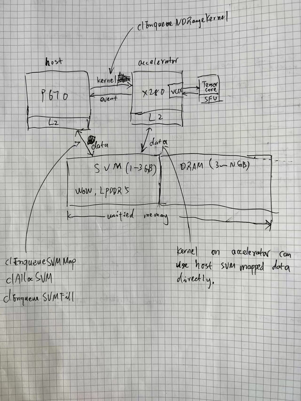
| SOPHGO TPU(Matrix) 16TOPs@INT8 and 8TFLOPs@BF16(FP16) | |
| Register-Level connection through VCIX with X280s | |
| GPU | IMG AXT-16-512 |
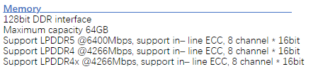
| Memory | 16G / 32G / 64G LPDDR5@6400Mbps, ECC, 128bit |
| Bandwidth | >100GB/s |
| Storage | Support UFS Module |
| 1x M.2 M Key 2280 Support NVMe SSD | |
| 1x micro SD card for recovery or OS loading | |
| 4x SATA | |
| Ethernet | 2x 1GbE RJ45,Configurable with 2x 25Gbps through PCIE |
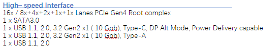
| USB | 2x USB 3.0 |
| 2x USB 2.0 | |
| 2x Front Panel USB 2.0 | |
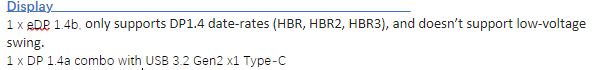
| 1x USB C with DP Alt Mode | |
| Display Engine | 2x HDMI 2.0 Out 4K@60fps, CEC and eARC |
| 1x eDP | |
| 1x TP (Touch Screen) | |
| 2 MIPI-DSI 2K@60fps | |
| Wireless | 1x M.2 B Key 3050 4G/WIFI/BT |
| TDP | 5W-30W |
| Price | 120 US Dollars - 200 US Dollars |
Vendor
SiFive
VCIX
SiFive Vector Coprocessor Interface (VCIX) Software Specification Version 1.0
LLVM vendor-extensions
IMG
Newsletter
- SG2380 will shine brilliantly on Second International workshop on RISC-V for HPC
- Sophgo SG2380 - A 2.5 GHz 16-core SiFive P670 RISC-V processor with a 20 TOPS AI accelerator - CNX Software
Attention
Availability and Pricing: The journey of the SG2380 SoC has officially begun. Expect the silicon to be at your fingertips in 9 months, and the Milk-V Oasis in just 10 months. An irresistible starting price of $120 awaits post coupon code application.
Secure Your Spot: Grab your coupon code and reserve the future of RISC-V desktops with our distributor, Arace Tech: Milk-V Oasis Pre-order .
There will be 4 different modes: Coupon(20% discount), Super Early Bird(15%), Early Bird(10%) and Kickstarter/CrowdSuppy Special(5%)
We welcome any suggestions regarding the SG2380, and any valuable suggestions that are adopted will be particularly beneficial for developers, making it a significant contribution to the open-source community! We will also offer early access privileges and small gifts.